Complete and validated design flow based on open-source tools
Foundry process and PDK
Prototyping services
Packaging options
Marketplace library of IP and reference design
Evaluate IP from the marketplace prior purchasing
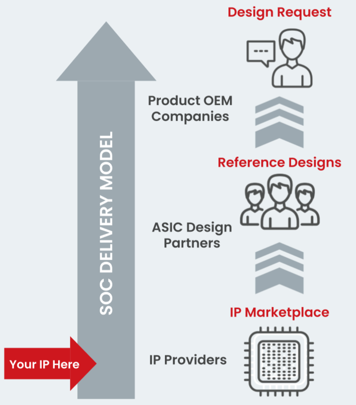
The Efabless Design Platform offers a complete IC development solution for design partners that streamlines the time and cost associated with creating custom silicon solutions.
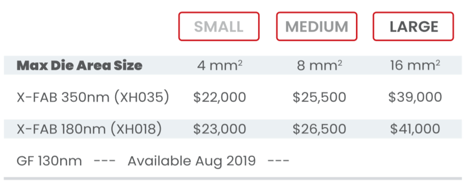
The design platform provides tools, infrastructures, Process and partnership required for a complete design and development of custom ASICs or IP. Fixed price packages are available based on maximum die area of the ASICs project and the node.
Pricing includes all design and development on the platform using the Efabless design flow
The pricing includes 50 samples(bare dies)
Prototyping is based on foundry prescheduled MPW shuttles. Contact us regarding upcoming shuttle dates and module support.
Packaging can be arranged through partners for and incremental cost.

 More info available online here.