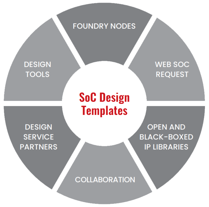
Leverage automated configurable design templates to rapidly generate your custom IC.
The first SoC design template is targeted for IoT Edge Devices optimized for cost, performance, power and size.

For Mature Nodes – the cost of development is driven by IP licenses, EDA tools and labor versus Silicon fabrication.
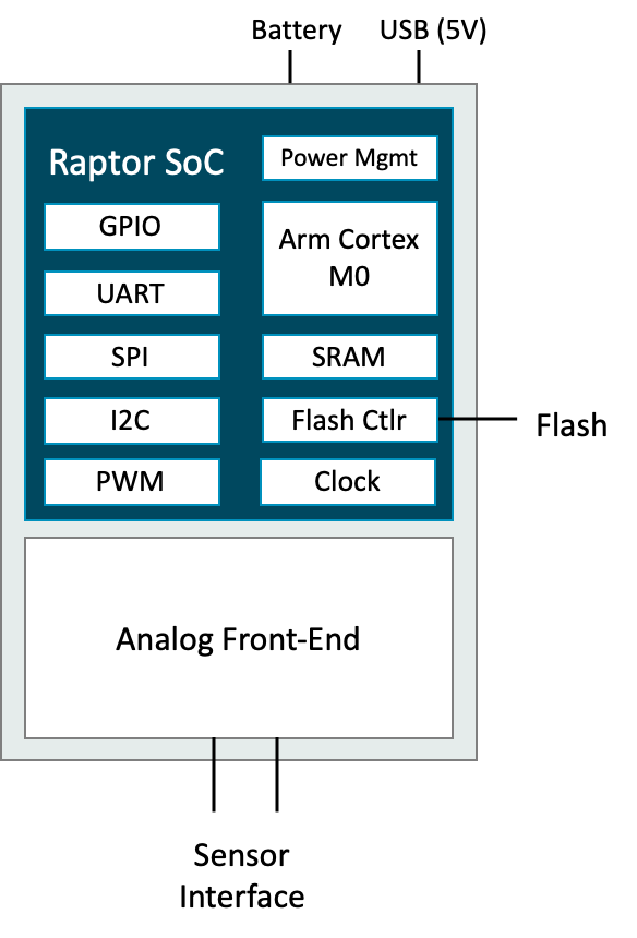
Combines custom analog front-end with configurable SoC design template
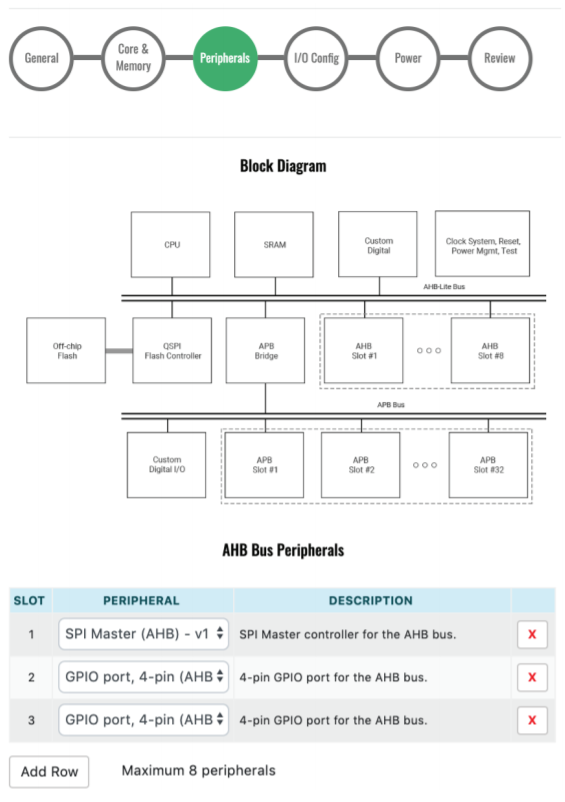
Custom SoC designs are automatically generated from a web-based UI using dropdown menus
Leverage Existing Designs and ExpertiseAllows you to create a full SoC without needing expertise for the full system design
FastDesigns are automatically generated along with software drivers and verification tests. Samples can be provided in as little as 20 weeks
Low NRE CostDesign time is reduced thru automated design generation. License fees for tools and IP are eliminated or deferred
Licensing costs for many IP are included as part of the solution
For IP with licensing costs, most are deferred until after initial samples
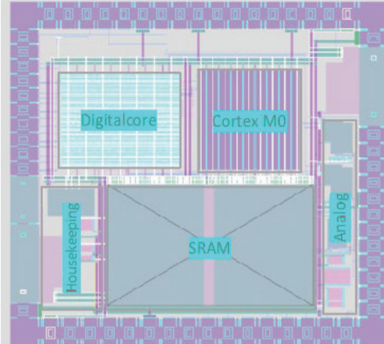
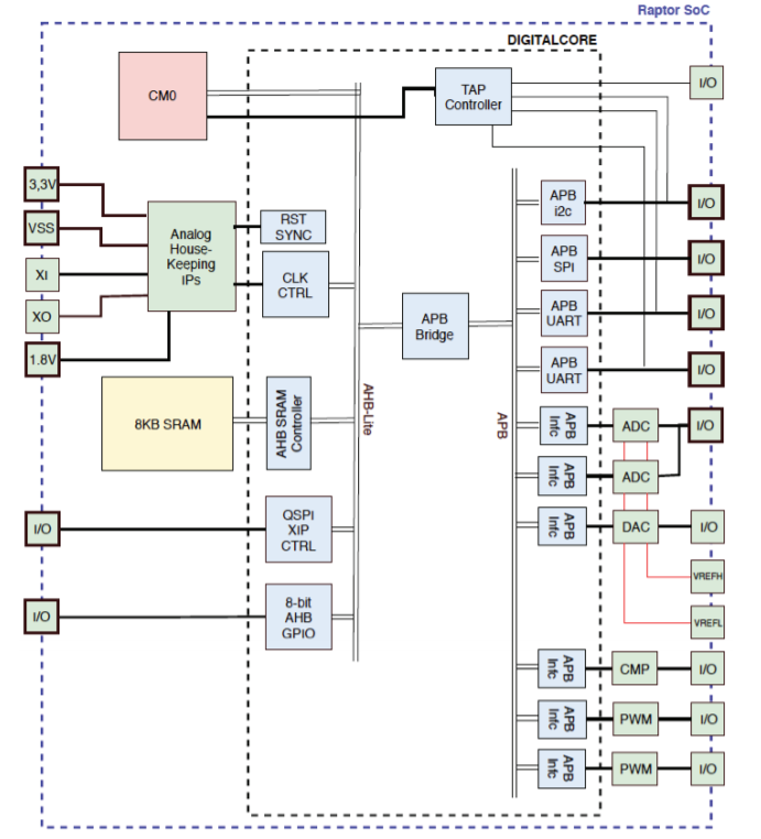
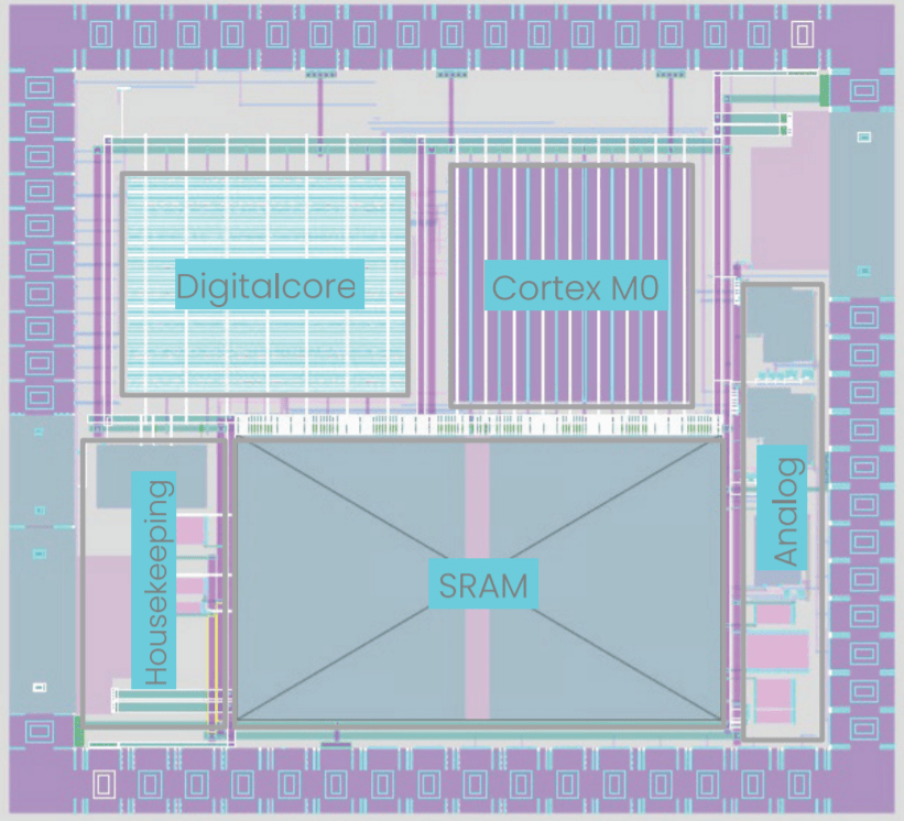
Mixed Signal Design with AnalogFull SoC / ASIC design capability including digital and analog devices
Custom Analog & Digital OptionsCustom analog and digital blocks can be requested and included to provide further customization
Open-source and Proprietary Designs / IPFlexibility to utilize and mix a growing portfolio of open-source and proprietary IP in your designs
Power can be optimized through pruning unused features and intelligent management of peripherals. Speed can be accelerated by moving from FPGA to hard implementations.
Cost can be reduced by moving from complex off-the-shelf parts as well as integration many discrete components.
Footprint is reduced through integration of discrete components into silicon and reducing board size.
Implementing critical functions or designs in silicon protects from reverse engineering by competitors.
Pricing incudes the delivery of 50 sample dies
Fabrication is based on scheduled foundry MPW shuttles
No IP licensing fees required for samples
Packaging included
EDA tool cost included -- Design Assisted and Roll-Your-Own services include use of EDA design flow on the Efabless platform
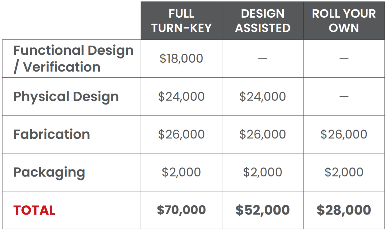
Dedicated shuttle pricing available upon request
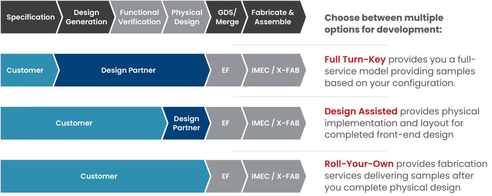
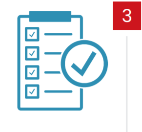
Getting samples for your custom SoC is made easy and fast through a streamlined process on the Efabless platform.

Create a custom configuration of an SoC using simple pulldown menus and a web-based wizard tool. Note any customization requirements.
Submit a request to Efabless to create samples. We will contact you to confirm your order and any additional requirements before proceeding.
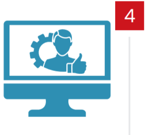
Get your SoC samples, either as packaged parts and/or on evaluation PCBAs. Use our example firmware to verify.
Transfer your design to a production mask. Lower upfront NRE by sharing mask and fabrication costs with other Efabless customers. Transition to an Efabless partner for long-term production and support.
Only what is available through configuration of the design template
Generated design can be further customized manually
New design templates will be added over time to address new application requirements
IP SelectionIP selection based on a silicon-proven pre-integrated IP library
Custom IP can be included for specific design templates & New IP will be added over time
Generated design can be further customized manually
Technology Nodes and FoundriesThe technology node is specified based on design template
New technology nodes and foundries to be added over time
Support for On-chip RF & FlashIP for on-chip RF and Flash are currently not available. Options to integrate RF and Flash are available through a SIP integrated solution
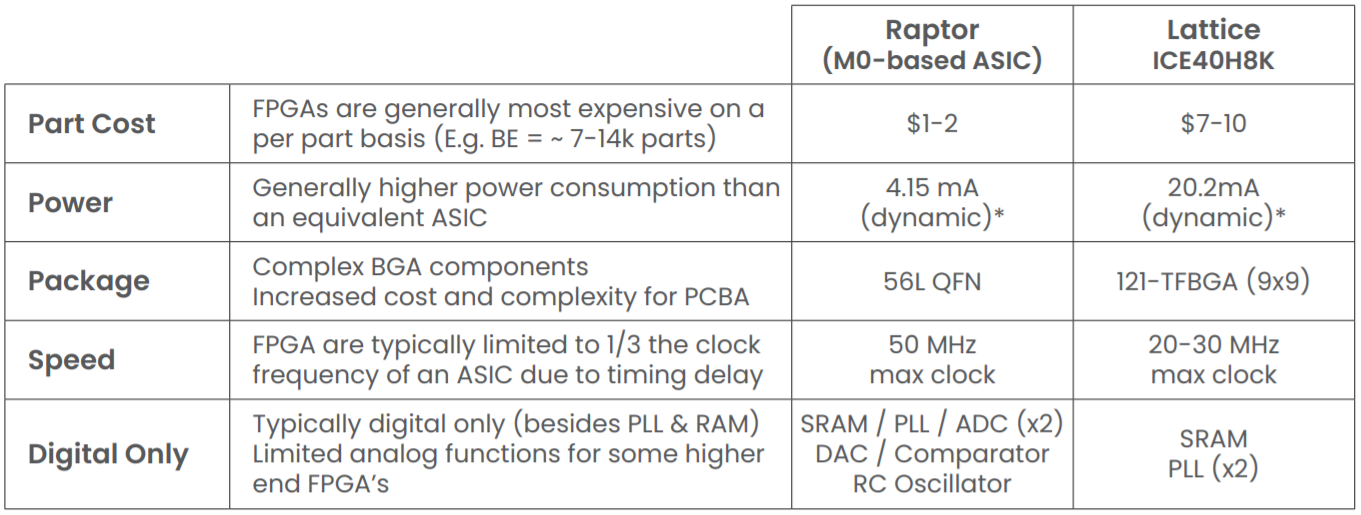 * Power calculations based on 32MHz clock and an activity factor of 0.1. FPGA is filled with 16-bit counters.
Efabless platform and marketplace opens the market for custom SoC creation and delivery